| CPC H01L 29/785 (2013.01) [H01L 21/823807 (2013.01); H01L 21/823814 (2013.01); H01L 21/823821 (2013.01); H01L 21/823871 (2013.01); H01L 27/0924 (2013.01); H01L 29/0847 (2013.01); H01L 29/1037 (2013.01); H01L 29/66795 (2013.01); H01L 2029/7858 (2013.01)] | 20 Claims |

|
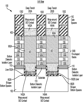
1. A semiconductor device structure comprising:
a first channel region over a substrate;
a second channel region over the first channel region;
a source or drain (S/D) trench having a S/D trench region and a bottom trench region;
a liner within the bottom trench region;
wherein the liner comprises a first liner element on a bottom surface of the bottom trench region;
wherein the liner further comprises a second liner element on sidewalls of the bottom trench region;
an under-contact spacer on the first liner element and along first portions of the second liner element such that second portions of the second liner element extend above the under-contact spacer;
a merged S/D region within the S/D trench region and adjacent to the first channel region and the second channel region, wherein the merged S/D region comprises a top surface, sidewalls, and a bottom surface; and
a wrap-around S/D contact configured such that a portion of the wrap-around S/D contact is between the bottom surface of the merged S/D region and a bi-layer bottom spacer comprising the liner and the under-contact spacer.
|