| CPC H01L 29/7848 (2013.01) [H01L 27/127 (2013.01); H01L 27/1266 (2013.01); H01L 29/78621 (2013.01); H01L 27/1218 (2013.01); H01L 29/0673 (2013.01); H01L 29/42392 (2013.01); H01L 29/785 (2013.01); H01L 29/78603 (2013.01); H01L 29/78696 (2013.01)] | 20 Claims |
|
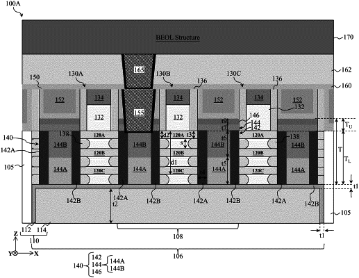
1. A semiconductor structure comprising:
a dielectric substrate; and
a channel layer, a gate disposed over the channel layer, and an epitaxial source/drain structure disposed adjacent to the channel layer, wherein the channel layer, the gate, and the epitaxial source/drain structure are disposed over the dielectric substrate, and further wherein the epitaxial source/drain structure includes:
an inner portion having a first dopant concentration, wherein the inner portion physically contacts the dielectric substrate, and
an outer portion having a second dopant concentration, wherein the second dopant concentration is less than the first dopant concentration and the outer portion is disposed between the inner portion and the channel layer.
|