| CPC H01L 29/7824 (2013.01) [H01L 29/0852 (2013.01); H01L 29/1033 (2013.01); H01L 29/66681 (2013.01)] | 20 Claims |
|
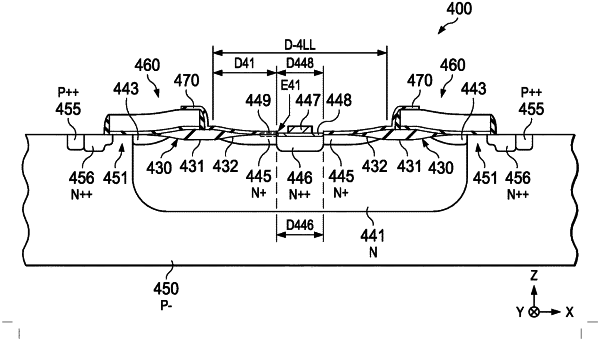
1. A semiconductor device, comprising:
a source region in a semiconductor substrate;
a drain region having a first conductivity type and a first dopant concentration spaced apart from the source region;
a first drift region located between the source region and the drain region and having the first conductivity type and a second dopant concentration that is lower than the first dopant concentration of the drain region;
a channel region having a different second conductivity type between the source region and the first drift region;
an oxide structure between the channel region and the drain region and including a first portion on or over the first drift region and a tapered portion between the first portion and the drain region;
a substrate surface extension between the tapered portion and the drain region;
a gate structure on or over the oxide structure and including a portion over the channel region; and
a buffer region having the first conductivity type between the first drift region and the drain region and under the tapered portion of the oxide structure, the buffer region having a third dopant concentration between the second dopant concentration of the drain region and the first dopant concentration of the first drift region.
|