| CPC H01L 29/7813 (2013.01) [H01L 29/1095 (2013.01); H01L 29/407 (2013.01); H01L 29/4236 (2013.01); H01L 29/42364 (2013.01); H01L 29/4991 (2013.01); H01L 29/66734 (2013.01); H01L 29/94 (2013.01)] | 7 Claims |
|
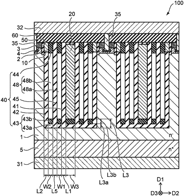
1. A semiconductor device, comprising:
a first electrode;
a first conductivity type first semiconductor region provided on the first electrode;
a second conductivity type second semiconductor region provided on the first semiconductor region;
a first conductivity type third semiconductor region selectively provided on the second semiconductor region;
a second electrode provided on the third semiconductor region and electrically connected to the third semiconductor region;
a third electrode aligned with the first semiconductor region and the second semiconductor region in a second direction perpendicular to a first direction from the first electrode toward the first semiconductor region;
a gate electrode provided between the third electrode and the second semiconductor region in the second direction;
a first insulating portion including a first insulating region provided between the third electrode and the first semiconductor region in the second direction and facing the third electrode in the second direction, a second insulating region facing the first semiconductor region in the second direction, and at least one air-gap region located between the first insulating region and the second insulating region in the second direction; and
a second insulating portion provided between the gate electrode and the second semiconductor region in the second direction,
a distance between the first electrode and a lower end of the third electrode being less than a distance between the first electrode and a lower end of the gate electrode, and
the first insulating region being located between the third electrode and the air-gap region in the second direction.
|