| CPC H01L 29/66969 (2013.01) [H01L 21/0234 (2013.01); H01L 21/0262 (2013.01); H01L 21/02326 (2013.01); H01L 21/02472 (2013.01); H01L 21/02483 (2013.01); H01L 21/02554 (2013.01); H01L 21/02565 (2013.01); H01L 21/02573 (2013.01); H01L 29/42384 (2013.01); H01L 29/4908 (2013.01); H01L 29/4966 (2013.01); H01L 29/7869 (2013.01); H01L 29/78621 (2013.01)] | 15 Claims |

|
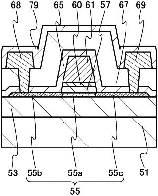
1. A method for manufacturing a semiconductor device including a transistor, the method comprising steps of:
forming an oxide semiconductor film;
forming a first insulating film over the oxide semiconductor film;
forming a metal oxide film over and in contact with the first insulating film;
performing a heat treatment after forming the metal oxide film;
forming a conductive film over the metal oxide film after performing the heat treatment; and
forming a second insulating film over the conductive film,
wherein a top surface of the oxide semiconductor film comprises a first region, a second region, and a third region between the first region and the second region,
wherein each of the first region and the second region is in contact with the second insulating film,
wherein the conductive film overlaps with the third region with the first insulating film and the metal oxide film therebetween,
wherein the second insulating film comprises hydrogen, and
wherein the metal oxide film and the conductive film are collectively configured to be a gate electrode of the transistor.
|