| CPC H01L 29/66568 (2013.01) [H01L 21/823814 (2013.01); H01L 21/823842 (2013.01); H01L 21/823878 (2013.01); H01L 21/823885 (2013.01); H01L 21/823892 (2013.01); H01L 27/088 (2013.01); H01L 27/092 (2013.01); H01L 27/0925 (2013.01); H01L 29/401 (2013.01); H01L 29/665 (2013.01)] | 12 Claims |
|
1. A method of microfabrication, the method comprising:
providing a substrate;
doping regions of the substrate by implanting a first dopant material;
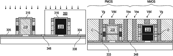
forming a layer stack on the substrate, the layer stack having a metal layer of a first metal positioned between a first dielectric layer and a second dielectric layer and a first capping layer on the second dielectric layer;
forming openings through the layer stack until uncovering the substrate;
depositing a high-K material in the openings;
removing the high-K material from horizontal surfaces of the layer stack and the substrate leaving the high-K material on walls of the openings;
epitaxially growing vertical channel structures in the openings for channels of transistors having current flow perpendicular to a working surface of the substrate;
depositing a high-K material on an upper surface of the vertical channel structures;
masking the substrate and etching the layer stack leaving sidewall structures of the layer stack on the vertical channel structures, the metal layer of the sidewall structures forming a gate contact of a field effect transistor;
masking the layer stack and the sidewall structures;
doping the substrate between the sidewall structures by implanting a second dopant material into the substrate; and
planarizing the substrate to remove the high-K material from the upper surface of the vertical channel structures.
|