| CPC H01L 29/66242 (2013.01) [H01L 21/762 (2013.01); H01L 21/76224 (2013.01); H01L 29/0603 (2013.01); H01L 29/0649 (2013.01); H01L 29/0821 (2013.01); H01L 29/1004 (2013.01); H01L 29/66272 (2013.01); H01L 29/7371 (2013.01); H01L 29/732 (2013.01)] | 20 Claims |

|
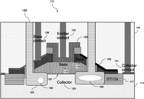
1. A method, comprising:
providing a substrate;
forming an NPN transistor comprising:
a collector region in the substrate,
a base region formed on the collector region, and
an emitter region formed on the base region;
forming a dielectric layer on the base region positioned laterally adjacent to the emitter region;
forming a trench extending through the dielectric layer and the base region and at least partially into the collector region so that the collector region is immediately adjacent to the trench, so that the base region is immediately adjacent to the trench, and so that the emitter region is separated from the trench; and
filling the trench with a core, the core being in contact with the collector region and the base region, being separated from the emitter region by at least a portion of the dielectric layer, and comprising a compressive material.
|