| CPC H01L 29/42392 (2013.01) [H01L 21/823412 (2013.01); H01L 21/823418 (2013.01); H01L 21/823468 (2013.01); H01L 21/823481 (2013.01); H01L 29/0649 (2013.01); H01L 29/6656 (2013.01); H01L 29/66742 (2013.01); H01L 29/78618 (2013.01); H01L 29/78696 (2013.01)] | 20 Claims |
|
1. A method, comprising:
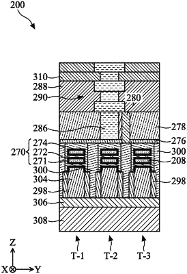
providing a workpiece including a frontside and a backside, the workpiece including a substrate, a first plurality of channel members over a first portion of the substrate, a second plurality of channel members over a second portion of the substrate, a first gate structure engaging the first plurality of channel members, a second gate structure engaging the second plurality of channel members, a dielectric fin disposed between the first and second gate structures, an isolation feature disposed under the dielectric fin and sandwiched between the first and second portions of the substrate, wherein the substrate is at the backside of the workpiece and the first and second pluralities of channel members are at the frontside of the workpiece;
forming a metal cap layer at the frontside of the workpiece, the metal cap layer electrically connecting the first and second gate structures;
depositing a dielectric feature on the dielectric fin, the dielectric feature dividing the metal cap layer into a first segment over the first gate structure and a second segment over the second gate structure;
etching the isolation feature, thereby forming a trench exposing the dielectric fin at the backside of the workpiece;
depositing a spacer layer on sidewalls of the trench;
etching the dielectric fin, thereby exposing a bottom surface of the dielectric feature in the trench; and
depositing a seal layer in the trench.
|