| CPC H01L 29/402 (2013.01) [H01L 21/02529 (2013.01); H01L 21/02634 (2013.01); H01L 21/26513 (2013.01); H01L 21/28537 (2013.01); H01L 21/3065 (2013.01); H01L 21/30625 (2013.01); H01L 21/324 (2013.01); H01L 29/401 (2013.01)] | 16 Claims |
|
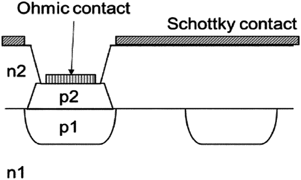
1. A method for manufacture of a grid structure in a SiC semiconductor material, the method comprising the steps of:
(a) providing a substrate comprising a doped semiconductor SiC material, the substrate comprising a first layer of a first conductivity type;
(b) by epitaxial growth adding at least one doped semiconductor SiC material to form separated second regions of a second conductivity type opposite to the first conductivity type on the first layer;
(c) by ion implantation at least once at a stage selected from the group consisting of after step (a) and after step (b), implanting ions in the first layer to form first regions of a second conductivity type opposite to the first conductivity type, wherein each of the separated second regions is in contact with one of the first regions; and
(d) by epitaxial growth, growing a second layer on the separated second regions and on the first layer.
|