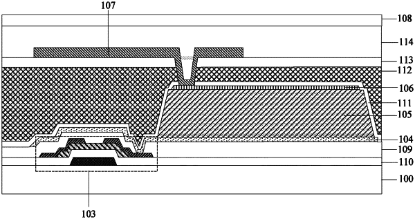
| CPC H01L 27/14612 (2013.01) [H01L 27/14663 (2013.01); H01L 27/14692 (2013.01)] | 16 Claims |

|
1. A detection substrate, comprising:
a base substrate;
a plurality of data lines extending along a first direction;
a plurality of gate lines extending along a second direction;
a plurality of thin film transistors arranged on the base substrate;
a plurality of first electrodes, a plurality of photoelectric conversion structures and a plurality of second electrodes arranged in sequence in a laminated manner and electrically connected with each other; and
a plurality of bias lines electrically connected with the plurality of second electrodes;
wherein each first electrode is electrically connected with a corresponding thin film transistor, and an orthographic projection of the each first electrode on the base substrate at least partially overlaps with an orthographic projection of an active layer of the corresponding thin film transistor on the base substrate; and
the each first electrode comprises a first protruding part arranged on a side, close to a corresponding data line, of the each first electrode, and an orthographic projection of the first protruding part on the base substrate is located between the orthographic projection of the active layer on the base substrate and an orthographic projection of the corresponding data line on the base substrate.
|