| CPC H01L 27/092 (2013.01) [H01L 21/266 (2013.01); H01L 21/26513 (2013.01); H01L 21/823814 (2013.01); H01L 21/823864 (2013.01); H01L 21/823878 (2013.01); H01L 29/4983 (2013.01); H01L 29/66492 (2013.01); H01L 29/7833 (2013.01)] | 20 Claims |

|
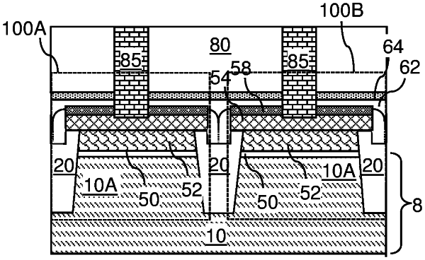
1. A semiconductor structure comprising:
first and second field effect transistors, wherein each of the first and second field effect transistors comprises:
a semiconductor active region including a source region, a channel region, and a drain region arranged along a first horizontal direction;
a gate dielectric contacting a top surface of the channel region;
a gate electrode overlying the gate dielectric; and
a pair of dielectric gate spacers located on opposite sides of the gate electrode; and
a shallow trench isolation structure which laterally surrounds each of the semiconductor active regions of the first and second two field effect transistors,
wherein each of the pair of dielectric gate spacers comprises:
over-active-region gate spacer portions overlying the semiconductor active regions and comprising straight inner sidewalls that are perpendicular to the first horizontal direction; and
inter-active-region gate spacer portions overlying portions of the shallow trench isolation structure and comprising stepped sidewalls including a lower straight sidewall segment adjoined to a respective pair of straight inner sidewalls, an upper straight sidewall segment that is laterally offset from the lower straight sidewall segment, and a connecting surface that is adjoined to a top edge of the lower straight sidewall segment and to a bottom edge of the upper straight sidewall segment.
|