| CPC H01L 27/0285 (2013.01) [H02H 9/046 (2013.01)] | 13 Claims |

|
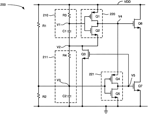
1. A voltage clamp, comprising:
a first transistor having a drain coupled to a power supply;
a second transistor having a drain coupled to a source of the first transistor and a source coupled to ground;
a third transistor configured to produce a positive feedback signal based on a first voltage at a gate of the second transistor;
a first inverter configured to control an operation of the first transistor based at least in part on the positive feedback signal so that the first transistor and the second transistor provide a discharge path between the power supply and ground;
a second inverter configured to produce the first voltage at the gate of the second transistor;
a voltage divider coupled between the power supply and ground and configured to provide a voltage divider output signal to an input of the second inverter; and
a first resistor-capacitor (RC) network coupled between the voltage divider and the second inverter, the first RC network being configured to filter the voltage divider output signal provided to the input of the second inverter.
|