| CPC H01L 24/85 (2013.01) [H01L 24/03 (2013.01); H01L 24/05 (2013.01); H01L 24/48 (2013.01); H01L 2224/03831 (2013.01); H01L 2224/04042 (2013.01); H01L 2224/48824 (2013.01); H01L 2224/85031 (2013.01); H01L 2224/85359 (2013.01)] | 6 Claims |

|
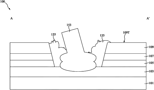
1. A method for preparing a semiconductor device, comprising:
providing an integrated circuit die having a bond pad;
forming a first dielectric layer over the bond pad;
forming a second dielectric layer over the first dielectric layer;
etching the first dielectric layer and the second dielectric layer to form a first opening exposing a top surface area of the bond pad;
partially recessing the top surface area of the bond pad to form a concave depression;
bonding a wire bond to the concave depression;
forming a first photoresist layer over the second dielectric layer, wherein the first opening is formed by using the first photoresist layer as a mask; and
forming a second photoresist layer over the first photoresist layer before the concave depression is formed.
|