| CPC H01L 24/81 (2013.01) [H01L 23/538 (2013.01); H01L 23/5381 (2013.01); H01L 23/5382 (2013.01); H01L 23/5389 (2013.01); H01L 24/11 (2013.01); H01L 24/14 (2013.01); H01L 2224/11462 (2013.01); H01L 2224/1403 (2013.01); H01L 2224/145 (2013.01); H01L 2224/14131 (2013.01)] | 6 Claims |

|
1. A method for fabricating a system-on-wafer structure, wherein the system-on-wafer structure comprises: a wafer substrate, an integrated chiplet, a system configuration board, and a thermal module,
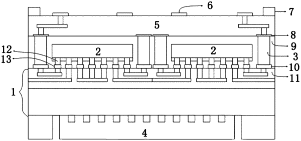
wherein a re-distributed layer is provided at the top of the wafer substrate, a bonding region formed by a wafer micro bump array is provided on an topside of the wafer substrate, a copper pillar array formed by connecting a copper pillar pad and a copper pillar is provided around the bonding region, a chiplet micro bump array is provided on a backside of the integrated chiplet and corresponds to the wafer micro bump array of the bonding region on the topside of the wafer substrate, a configuration controller and a connector are integrated on the system configuration board, and a pad is provided on a backside of the system configuration board, the system configuration board is a Printed Circuit Board (PCB) board, the configuration controller is configured for power supplying, testing and system configuration of the integrated chiplet, the wafer substrate and the integrated chiplet are bonded in the bonding region through the wafer micro bump array and the chiplet micro bump array, the wafer substrate and the system configuration board are bonded through the copper pillar array and the pad, a molding layer is provided between the wafer substrate and the system configuration board, and is configured to mold the wafer substrate, the integrated chiplet bonded to the wafer substrate, and the copper pillar array, each integrated chiplet is electrically connected to each other through the re-distributed layer, the system configuration board is electrically connected to the integrated chiplet through the re-distributed layer and the copper pillar array, and the system thermal module is attached to a lower surface of the wafer substrate, and
wherein the method comprises:
step S1, performing multiple patterning operations on the wafer substrate to form a plurality of primary patterning regions on the surface of the wafer substrate, wherein the patterning operations comprise: forming the re-distributed layer, the wafer micro bump array and the copper pillar gasket at the top of the wafer substrate through a semiconductor front-end/back-end metal process, and wherein the bonding region on the wafer substrate is formed by the wafer micro bump array;
step S2, bonding the integrated chiplet with the wafer substrate through a Chip to Wafer (C2 W) bonding process to from an integrated wafer;
step S3, depositing a thick photoresist film on the top of an integrated wafer with a thickness greater than or equal to 100 μm, and etching the thick photoresist film to form a deep hole for cupper pillar deposition;
step S4, forming the copper pillar at the copper pillar hole etched in the step S3 through an electroplating process;
step S5, removing the photoresist, molding the integrated wafer to form the molding layer, and thinning the molding layer to reveal the copper pillar; and
step S6, aligning and bonding the copper pillar with the pad on the backside of the system configuration board, and attaching the system thermal module at a bottom of the integrated wafer to complete the system-on-wafer structure.
|