| CPC H01L 24/13 (2013.01) [H01L 21/027 (2013.01); H01L 24/04 (2013.01); H01L 24/11 (2013.01); H01L 2221/1068 (2013.01); H01L 2224/022 (2013.01); H01L 2224/0401 (2013.01); H01L 2224/1146 (2013.01); H01L 2224/1147 (2013.01); H01L 2224/13144 (2013.01); H01L 2224/13147 (2013.01); H01L 2924/014 (2013.01); H01L 2924/177 (2013.01)] | 17 Claims |
|
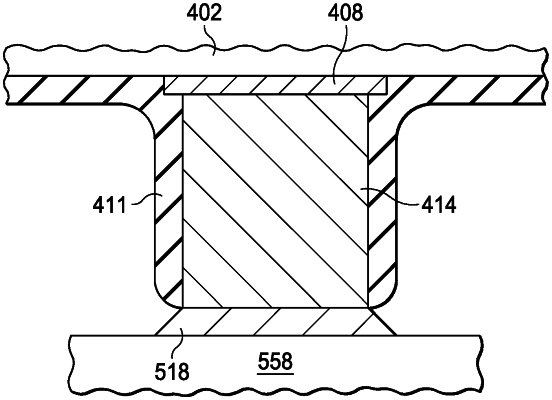
1. An apparatus, comprising:
a semiconductor die having a device side surface;
bond pads on the semiconductor die on the device side surface;
post connects having a proximate end on the bond pads and extending from the bond pads to a distal end, the diameter of the post connects including a uniform diameter from the proximate end to the distal end;
polyimide material covering sides of the post connects from the proximate end till the distal end, and covering at least a portion of the bond pads;
solder on the distal end of the post connects; and
a portion of a lead frame physically contacting the solder.
|