| CPC H01L 23/645 (2013.01) [H01F 27/2804 (2013.01); H01L 28/10 (2013.01); H01F 2027/2809 (2013.01)] | 18 Claims |
|
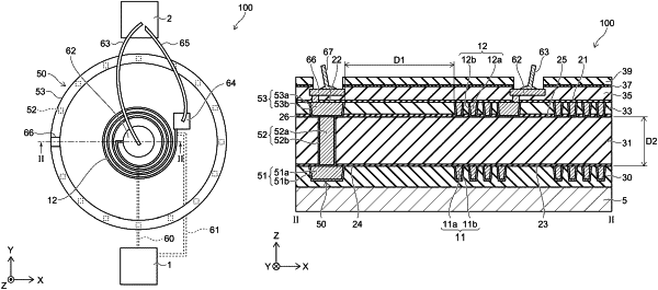
1. An isolator, comprising:
a first electrode electrically connected to a reference potential;
a second electrode provided on the first electrode and separated from the first electrode;
a first pad provided on one end of the second electrode and electrically connected to the one end of the second electrode;
a second pad provided on other end of the second electrode and electrically connected to the other end of the second electrode;
a conductive body provided around the first and second electrodes along a first plane perpendicular to a first direction, the first direction being from the first electrode toward the second electrode, the conductive body being electrically connected to the reference potential; and
a first insulating region provided on the second electrode, the first insulating region including silicon, carbon, and nitrogen, the first insulating region directly contacting an upper surface of the second electrode, and the first insulating region covering whole area of the upper surface of the second electrode except the one end and the other end of the second electrode,
a second insulating portion provided between the second electrode and the conductive body,
the first insulating region directly contacting an upper surface of the second insulating portion,
wherein a maximum concentration of a metal at an interface between the second insulating portion and the first insulating region is no more than 100 times a minimum concentration of copper in the second insulating portion and the first insulating region.
|