| CPC H01L 23/576 (2013.01) [H01L 29/0843 (2013.01); H01L 29/78 (2013.01); H03K 3/0315 (2013.01); H10B 10/12 (2023.02)] | 20 Claims |
|
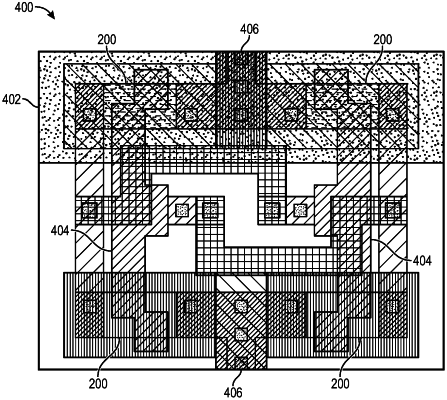
1. A field-effect transistor for a physical unclonable function (PUF) circuit comprising:
a split source and drain configuration comprising:
a source region including at least one source surface inflection segment disposed on an inner surface of the source region; and
a drain region disposed adjacent to the source region and separated from the source region by a channel, the drain region including at least one drain surface inflection segment disposed on an inner surface of the drain region, the at least one drain surface inflection segment protruding into the channel,
wherein the at least one source surface inflection segment protrudes into the channel,
wherein the at least one drain surface inflection segment is offset from the at least one source surface inflection segment along a length of the channel, and
wherein the at least one source surface inflection segment and the at least one drain surface inflection segment increase corner effects to thereby increase a manufacturing variability of the field-effect transistor.
|