| CPC H01L 23/564 (2013.01) [H01L 24/03 (2013.01); H01L 24/05 (2013.01); H01L 24/13 (2013.01); H01L 2224/0346 (2013.01); H01L 2224/0391 (2013.01); H01L 2224/0401 (2013.01); H01L 2224/05024 (2013.01); H01L 2224/13026 (2013.01); H01L 2924/05042 (2013.01); H01L 2924/07025 (2013.01)] | 15 Claims |
|
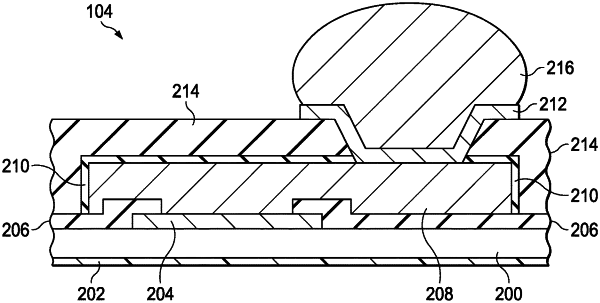
1. A semiconductor package, comprising:
a semiconductor die;
a passivation layer abutting a device side of the semiconductor die;
a first conductive layer abutting the device side of the semiconductor die;
a second conductive layer the passivation layer and physically contacting the first conductive layer;
a silicon nitride layer abutting the second conductive layer; and
a third conductive layer coupled to the second conductive layer at a gap in the silicon nitride layer, the third conductive layer configured to receive a solder ball.
|