| CPC H01L 23/562 (2013.01) [H01L 21/7602 (2013.01); H01L 21/76232 (2013.01)] | 4 Claims |
|
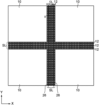
1. A semiconductor device comprising:
a semiconductor substrate formed of silicon carbide with a 4H—SiC crystal structure, components being formed at one surface of the semiconductor substrate, and the semiconductor substrate being formed in a rectangular shape in plan view;
a periphery portion disposed at a pre-specified region of a periphery of the semiconductor substrate, the components not being formed at the periphery portion; and
a plurality of trenches or portions of trenches formed at the periphery portion, each of the trenches being formed in a polygonal shape in plan view,
wherein a side of the semiconductor substrate in one direction is parallel with a direction of a crystal axis of the crystal structure, and at least one side in plan view of each of the trenches is orthogonal to the direction of the crystal axis.
|