| CPC H01L 23/5384 (2013.01) [H01L 23/5386 (2013.01); H01L 25/0657 (2013.01)] | 18 Claims |

|
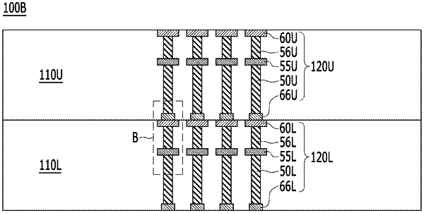
1. A semiconductor die bonding structure, comprising:
a lower die including a lower top bonding dielectric layer and lower connection structures; and
an upper die stacked over the lower die in a vertical direction and including an upper bottom bonding dielectric layer and upper connection structures,
wherein:
the lower top bonding dielectric layer and the upper bottom bonding dielectric layer are directly bonded to each other,
each of the lower connection structures includes a lower top bonding pad structure having a first width in a first horizontal direction and a second width in a second horizontal direction,
each of the upper connection structures includes an upper bottom bonding pad structure having a third width in the first horizontal direction and a fourth width in the second horizontal direction;
the first horizontal direction, the second horizontal direction, and the vertical direction are substantially perpendicular to one another,
the second width is greater than the first width, and
the second width is greater than the fourth width.
|