| CPC H01L 23/528 (2013.01) [H01L 21/76816 (2013.01)] | 9 Claims |
|
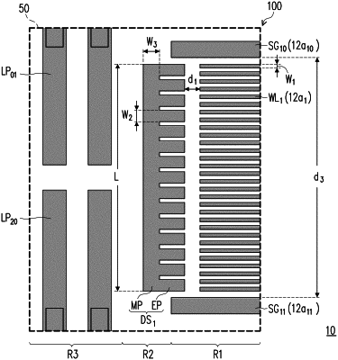
1. A memory device, comprising:
a substrate;
a plurality of word lines, extending in a first direction, arranged in a second direction, and disposed on the substrate;
a dummy structure, adjacent to ends of the word lines, and disposed on the substrate, wherein the dummy structure comprises:
a main part, extending in the second direction;
a plurality of extension parts, extending in the first direction, connected to the main part, and interposed between the main part and the word lines; and
a plurality of landing pads extending in the second direction and respectively connected to a plurality of other word lines, wherein the dummy structure is disposed between the landing pads and the word lines.
|