| CPC H01L 23/528 (2013.01) [H01L 21/31116 (2013.01); H01L 21/762 (2013.01); H01L 21/76802 (2013.01); H01L 21/76877 (2013.01); H01L 23/535 (2013.01); H01L 23/53295 (2013.01); H01L 29/0649 (2013.01); H10B 41/10 (2023.02); H10B 41/35 (2023.02); H10B 41/40 (2023.02); H10B 43/10 (2023.02); H10B 43/35 (2023.02); H10B 43/40 (2023.02); H10B 63/30 (2023.02); H10B 63/845 (2023.02); H10N 70/231 (2023.02); H10N 70/25 (2023.02); H10N 70/823 (2023.02); H10B 41/27 (2023.02); H10B 43/27 (2023.02); H10B 63/34 (2023.02)] | 16 Claims |

|
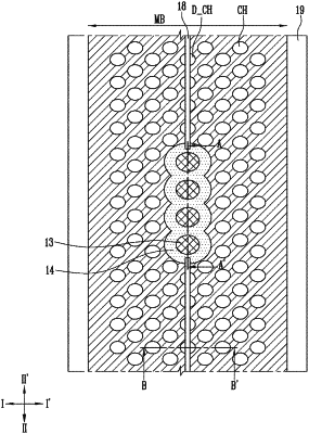
1. A semiconductor device, comprising:
a wiring structure;
a stacked structure formed over the wiring structure;
channel structures passing through the stacked structure;
contact plugs passing through the stacked structure, the contact plugs being electrically connected to the wiring structure;
insulating spacers, each including loop patterns surrounding a sidewall of each contact plug and stacked along the sidewall of each contact plug; and
an isolation pattern passing through a portion of the stacked structure,
wherein the loop patterns include:
a first loop pattern contacting the isolation pattern; and
a second loop pattern contacting the stacked structure and protruding more than the first loop pattern.
|