| CPC H01L 23/49816 (2013.01) [H01L 21/4853 (2013.01); H01L 21/56 (2013.01); H01L 23/3185 (2013.01); H01L 23/49822 (2013.01); H01L 24/11 (2013.01); H01L 24/73 (2013.01); H01L 25/0657 (2013.01); H01L 25/18 (2013.01); H01L 25/50 (2013.01); H01L 2224/73253 (2013.01)] | 20 Claims |

|
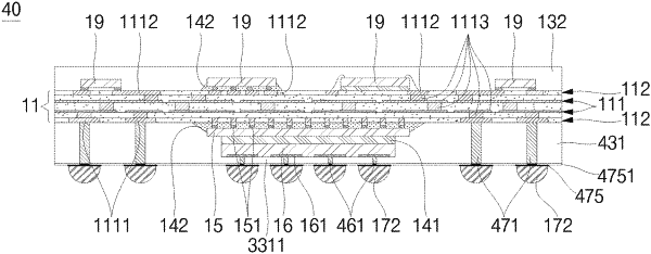
1. A semiconductor device, comprising:
a substrate comprising a substrate top side, an opposing substrate bottom side, and a conductive structure, wherein:
the conductive structure comprises:
substrate top terminals adjacent to the substrate top side;
substrate bottom terminals adjacent to the substrate bottom side; and
conductive paths coupling the substrate top terminals to the substrate bottom terminals;
a first electronic component comprising:
a first electronic component first side;
a first electronic component second side opposite to the first electronic component first side; and
first component terminals adjacent to the first electronic component first side and coupled to the substrate bottom terminals;
a second electronic component comprising:
a second electronic component first side;
a second electronic component second side opposite to the second electronic component first side and coupled to the first electronic component second side with an attachment structure; and
second component terminals adjacent to the second electronic component first side;
interconnects coupled to the substrate bottom terminals; and
a bottom encapsulant covering the substrate bottom side, the first electronic component, the second electronic component, the attachment structure, and the interconnects;
wherein:
the first electronic component and the second electronic component are interposed between the second component terminals and the substrate bottom side;
distal ends of the interconnects and distal ends of the second component terminals are substantially coplanar;
the bottom encapsulant and the attachment structure are different materials; and
portions of the second component terminals and the interconnects are exposed from the bottom encapsulant.
|