| CPC H01L 23/481 (2013.01) [H01L 23/5226 (2013.01); H01L 23/5283 (2013.01); H01L 24/06 (2013.01); H01L 25/18 (2013.01); H01L 2224/0401 (2013.01); H01L 2224/06182 (2013.01)] | 11 Claims |

|
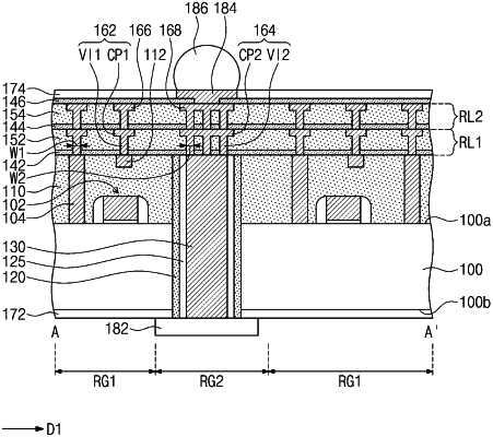
1. A semiconductor device, comprising:
a substrate provided with an integrated circuit and a contact electrically connected to the integrated circuit;
an interlayer dielectric layer on the substrate, the interlayer dielectric layer covering the integrated circuit and the contact;
a through electrode penetrating the substrate and the interlayer dielectric layer;
a first intermetal dielectric layer on the interlayer dielectric layer; and
a first wiring pattern and a second wiring pattern in the first intermetal dielectric layer,
wherein the first wiring pattern includes:
a first conductive pattern on the through electrode; and
a first via vertically penetrating the first intermetal dielectric layer and connecting the first conductive pattern to the through electrode,
wherein the first via is interposed between the first conductive pattern and the through electrode,
wherein the second wiring pattern includes:
a second conductive pattern on the contact; and
a second via vertically penetrating the first intermetal dielectric layer and connecting the second conductive pattern to the contact, and
wherein a first width, in a first direction, of the first via is greater than a second width, in the first direction, of the second via, the first direction being parallel to a top surface of the interlayer dielectric layer.
|