| CPC H01L 23/3738 (2013.01) [H01L 23/3736 (2013.01); H01L 24/08 (2013.01); H01L 24/13 (2013.01); H01L 25/0657 (2013.01); H01L 25/18 (2013.01); H01L 25/50 (2013.01); H01L 24/05 (2013.01); H01L 24/24 (2013.01); H01L 29/7371 (2013.01); H01L 2224/05644 (2013.01); H01L 2224/08145 (2013.01); H01L 2224/1357 (2013.01); H01L 2224/13147 (2013.01); H01L 2224/13644 (2013.01); H01L 2224/24146 (2013.01)] | 20 Claims |
|
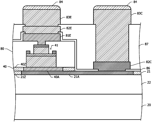
1. A semiconductor device comprising:
a substrate including a surface layer portion configured of a semiconductor material;
a bond layer disposed on the surface layer portion of the substrate and including at least one metal region in a plan view;
at least one semiconductor element disposed on the bond layer, the at least one semiconductor element including at least one first transistor disposed on a first metal region that is a metal region serving as the at least one metal region of the bond layer, and the first transistor including a collector layer electrically coupled to the first metal region, a base layer disposed on the collector layer, and an emitter layer disposed on the base layer,
a first emitter electrode disposed on the emitter layer of the first transistor and electrically coupled to the emitter layer; and
a first conductor protrusion disposed above the first emitter electrode, electrically coupled to the first emitter electrode, and protruding in a direction of going away from the substrate,
thermal conductivity of the semiconductor material of the surface layer portion of the substrate being higher than thermal conductivity of each of the collector layer, the base layer, and the emitter layer of the first transistor.
|