| CPC H01L 21/76897 (2013.01) [H01L 21/26586 (2013.01); H01L 21/3086 (2013.01); H01L 21/32139 (2013.01); H01L 29/401 (2013.01); H01L 29/41741 (2013.01); H01L 29/4236 (2013.01); H01L 29/66666 (2013.01); H01L 29/7827 (2013.01); H01L 29/105 (2013.01); H01L 29/7813 (2013.01)] | 11 Claims |

|
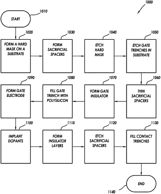
1. A method of fabricating a semiconductor device on a substrate, comprising:
forming hard mask pillars on a surface of the substrate;
forming sacrificial spacers on a first side of each hard mask pillar and a second side of each hard mask pillar, wherein open gaps are formed between adjacent sacrificial spacers;
etching the hard mask pillars to form pillar gaps;
etching gate trenches into the substrate through the open gaps and the pillar gaps;
forming a gate electrode within the gate trenches;
implanting channels and sources in the substrate below the sacrificial spacers;
forming an insulator layer around the sacrificial spacers;
etching the sacrificial spacers to form contact trenches within the substrate; and
filling the contact trenches with a conductive material to form contacts.
|