| CPC H01L 21/76895 (2013.01) [H01L 21/76802 (2013.01); H01L 21/76843 (2013.01); H01L 21/76877 (2013.01); H01L 21/76885 (2013.01)] | 19 Claims |

|
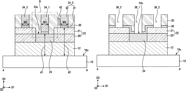
1. A method of forming an integrated circuit device, the method comprising:
forming a first insulating layer and a via contact on a substrate, wherein the substrate comprises an upper surface facing the via contact, and the via contact is in the first insulating layer and comprises a lower surface facing the substrate and an upper surface opposite to the lower surface; and
forming a second insulating layer, a first metallic wire on the via contact, and a second metallic wire on the first insulating layer, wherein the first metallic wire is in the second insulating layer and comprises a lower surface that faces the substrate and contacts the upper surface of the via contact,
wherein both the lower surface of the first metallic wire and an interface between the first metallic wire and the via contact have a first width in a first horizontal direction that is parallel to the upper surface of the substrate,
wherein the first metallic wire and the second metallic wire are spaced apart from each other, and a portion of the second insulating layer separates the first metallic wire from the second metallic wire,
wherein the lower surface of the first metallic wire is spaced apart from the substrate by a first distance in a third direction intersecting in the first horizontal direction,
wherein a lower surface of the second metallic wire is spaced apart from the substrate by a second distance in the third direction, and
wherein the second distance is longer than the first distance.
|