| CPC H01L 21/76232 (2013.01) [H01L 21/32134 (2013.01); H01L 21/32135 (2013.01); H01L 21/32139 (2013.01); H01L 21/76224 (2013.01); H01L 21/823481 (2013.01); H01L 21/823821 (2013.01); H01L 21/823878 (2013.01); H01L 27/088 (2013.01); H01L 29/4011 (2019.08); H01L 29/785 (2013.01); H01L 21/823437 (2013.01); H01L 29/66795 (2013.01)] | 20 Claims |
|
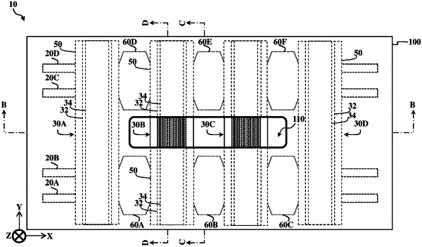
1. A semiconductor device comprising:
a first gate stack and a second gate stack disposed in a first dielectric layer, wherein the first gate stack interposes first source/drain features and the second gate stack interposes second source/drain features along a first direction; and
a gate isolation structure disposed in the first dielectric layer, wherein the gate isolation structure interposes the first gate stack and the second gate stack along a second direction that is different than the first direction, and further wherein the gate isolation structure includes:
a first spacer and a second spacer abutting the first dielectric layer,
a second dielectric layer abutting the first spacer,
a third dielectric layer abutting the second spacer,
a fourth dielectric layer between the second dielectric layer and the third dielectric layer.
|