| CPC H01L 21/4842 (2013.01) [H01L 21/561 (2013.01); H01L 21/78 (2013.01); H01L 23/3107 (2013.01); H01L 23/49805 (2013.01); H01L 24/48 (2013.01); H01L 21/4839 (2013.01); H01L 2224/48245 (2013.01)] | 17 Claims |

|
1. A method for fabricating semiconductor packages from a package assembly comprising:
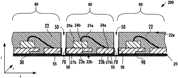
providing a lead frame assembly comprising a plurality of leads adjacently positioned, each lead comprising a first surface and a second surface;
encapsulating portions of the lead frame assembly in a mold encapsulation such that the second surface of each of the plurality of leads remain exposed, the mold encapsulation having a first major surface and a second major surface;
plating the second surface of each of the plurality of leads with a first electrical plating;
applying a conductive film across the second surface of each of the plurality of leads and the second major surface of the mold encapsulation;
cutting in a first direction through the mold encapsulation, each of the plurality of leads, and the first electrical plating on the second surface of each of the plurality of leads to create a channel in each of the plurality of leads, each of the channels exposing a first lead sidewall and a second lead sidewall of each of the plurality of leads;
plating, through the channel, the first lead sidewall and the second lead sidewall of each of the plurality of leads with a second electrical plating; and
removing the conductive film.
|