US 11,875,989 B2
Semiconductor device, solid-state imaging device and electronic apparatus
Taku Umebayashi, Kanagawa (JP); Keiji Tatani, Kanagawa (JP); Hajime Inoue, Kanagawa (JP); and Ryuichi Kanamura, Kumamoto (JP)
Assigned to SONY GROUP CORPORATION, Tokyo (JP)
Filed by SONY GROUP CORPORATION, Tokyo (JP)
Filed on Apr. 13, 2022, as Appl. No. 17/719,554.
Application 17/719,554 is a continuation of application No. 17/068,783, filed on Oct. 12, 2020, granted, now 11,374,049.
Application 17/068,783 is a continuation of application No. 16/555,067, filed on Aug. 29, 2019, granted, now 10,840,290, issued on Nov. 17, 2020.
Application 16/555,067 is a continuation of application No. 16/373,105, filed on Apr. 2, 2019, granted, now 10,475,845, issued on Nov. 12, 2019.
Application 16/373,105 is a continuation of application No. 16/042,094, filed on Jul. 23, 2018, granted, now 10,535,700, issued on Jan. 14, 2020.
Application 16/042,094 is a continuation of application No. 15/852,468, filed on Dec. 22, 2017, granted, now 10,128,301, issued on Nov. 13, 2018.
Application 15/852,468 is a continuation of application No. 15/403,154, filed on Jan. 10, 2017, granted, now 9,917,131, issued on Mar. 13, 2018.
Application 15/403,154 is a continuation of application No. 15/087,894, filed on Mar. 31, 2016, granted, now 9,570,499, issued on Feb. 14, 2017.
Application 15/087,894 is a continuation of application No. 14/434,288, granted, now 9,431,450, issued on Aug. 30, 2016, previously published as PCT/US2013/006055, filed on Oct. 10, 2013.
Claims priority of application No. 2012-230805 (JP), filed on Oct. 18, 2012; and application No. 2013-089580 (JP), filed on Apr. 22, 2013.
Prior Publication US 2022/0246668 A1, Aug. 4, 2022
Int. Cl. H01L 27/146 (2006.01)
CPC H01L 27/14645 (2013.01) [H01L 27/1464 (2013.01); H01L 27/1469 (2013.01); H01L 27/14612 (2013.01); H01L 27/14621 (2013.01); H01L 27/14623 (2013.01); H01L 27/14627 (2013.01); H01L 27/14634 (2013.01); H01L 27/14636 (2013.01); H01L 27/14643 (2013.01)] 20 Claims
OG exemplary drawing
 
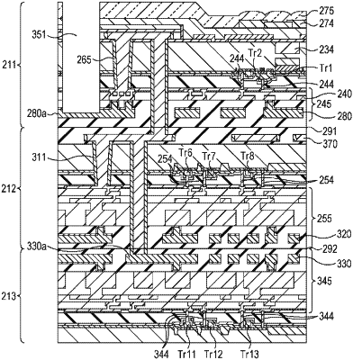
1. A light detecting device, comprising:
a first section including a first substrate and a first wiring layer;
a second section including a second substrate, a second wiring layer, and a third wiring layer;
a third section including a third substrate and a fourth wiring layer; and
an electrode pad,
wherein the first section, the second section, and the third section are stacked such that the first wiring layer and the second wiring layer face each other, and the third wiring layer and the fourth wiring layer face each other,
wherein the first section and the second section are electrically connected to each other, and the second section and the third section are electrically connected to each other,
wherein the second wiring layer and the third wiring layer are electrically connected to each other by a first contact, and
wherein a surface of the electrode pad facing away from the third section is exposed.