| CPC H01J 37/32963 (2013.01) [H01L 21/3065 (2013.01); H01L 21/31116 (2013.01); H01L 22/26 (2013.01); H01J 2237/334 (2013.01)] | 15 Claims |

|
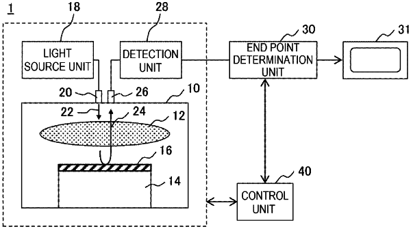
1. A plasma processing apparatus that performs, on a wafer in which a multilayer film in which an insulating film and a film to be processed containing a metal are alternately laminated is formed on a substrate, plasma etching of the film to be processed, the plasma processing apparatus comprising:
a processing chamber which is disposed inside a vacuum container;
a sample stage which is disposed inside the processing chamber and on which the wafer is placed;
a detection unit which detects reflected light obtained by the wafer reflecting light emitted to the wafer;
a control unit which controls plasma processing on the wafer; and
an end point determination unit which determines an etching end point of the film to be processed based on a change in an amplitude of vibration in a wavelength direction of a light spectrum of the reflected light, wherein
the control unit receives determination of the endpoint made by the end point determination unit and stops the plasma processing on the wafer.
|