| CPC G11C 16/30 (2013.01) [G01R 31/3177 (2013.01); G11C 16/14 (2013.01); G11C 16/26 (2013.01); H02M 3/073 (2013.01); H02M 3/071 (2021.05)] | 20 Claims |
|
1. A memory device, comprising:
a plurality of sub-arrays;
a charge pump architecture, comprising:
a number of pump stages for increasing a value of an input voltage and obtaining an overvoltage output value to be provided to a selected one or more of the plurality of sub-arrays; and
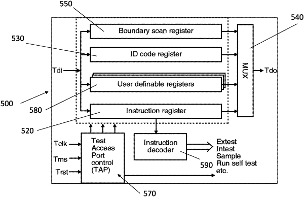
a registers block comprising:
a pump address register indicating an address of the selected one or more of the plurality of sub-arrays; and
a number of registers storing values corresponding to respective target overvoltage characteristics, wherein the stored values correspond to a particular operation type to be performed on the selected one or more of the plurality of sub-arrays.
|