| CPC G11C 13/004 (2013.01) [G11C 13/0004 (2013.01); G11C 13/0026 (2013.01); G11C 13/0028 (2013.01); G11C 2013/0054 (2013.01); G11C 2213/72 (2013.01)] | 28 Claims |

|
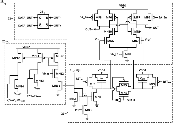
1. A sense circuit for use with an array of memory cells, the sense circuit comprising:
a regulation circuit configured to receive as input an input voltage, a full read voltage from reading of a selected cell of the array of memory cells, and a fractional read voltage applied to unselected cells of the array of memory cells, the regulation circuit configured to generate a regulated voltage and a regulated fractional voltage based upon the input, wherein the regulated voltage and the regulated fractional voltage are used in reading of the selected cell of the array of memory cells;
a capacitor circuit configured to generate a reference voltage through charge sharing between an input capacitor and a reference capacitor; and
a comparator circuit configured to generate a data output signal based upon a comparison between the reference voltage and the input voltage.
|