| CPC G11C 11/419 (2013.01) [G11C 11/418 (2013.01)] | 20 Claims |
|
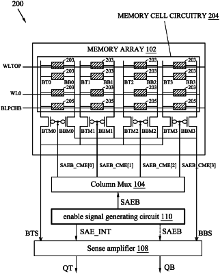
1. A memory device, comprising:
a memory array;
a column selection circuit coupled to the memory array, wherein the column selection circuit is configured to generate a column selection signal;
a sense amplifier configured to receive data signals from the memory array; and
an enable signal generating circuit including a logic gate and an inverter having an input coupled to an output of the logic gate, wherein:
the logic gate is configured to receive an input enable signal at an input thereof and to generate a first enable signal at the output thereof;
the inverter is configured to generate a second enable signal at an output thereof;
the column selection circuit is coupled to the output of the logic gate and is configured to generate the column selection signal based on the first enable signal; and
the sense amplifier is configured to receive a data signal from the memory array in response to the first enable signal and the second enable signal.
|