| CPC G09G 3/3648 (2013.01) [G09G 2300/0842 (2013.01); G09G 2320/0214 (2013.01)] | 18 Claims |

|
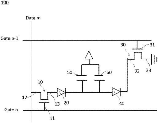
1. A pixel drive circuit, comprising: a first thin film transistor, a first unidirectional conduction switch connected in series with the first thin film transistor, a second thin film transistor, a second unidirectional conduction switch connected in series with the second thin film transistor, and a pixel capacitor arranged between the first unidirectional conduction switch and the second unidirectional conduction switch;
wherein the first thin film transistor comprises: a first gate electrode, a first source electrode, and a first drain electrode; the first gate electrode being connected with a n-th scan line, the first source electrode being connected with a m-th scan line, and the first drain electrode being connected with the pixel capacitor, and the n and m are positive integers; and
the second thin film transistor comprises: a second gate electrode, a second source electrode, and a second drain electrode; the second gate electrode being connected with a (n−1)-th scan line, the second source electrode being connected with the pixel capacitor, and the second drain electrode being grounded.
|