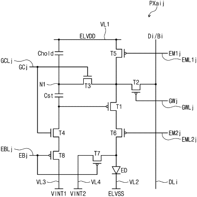
| CPC G09G 3/3233 (2013.01) [G09G 2300/0819 (2013.01); G09G 2300/0842 (2013.01); G09G 2300/0852 (2013.01); G09G 2300/0861 (2013.01); G09G 2310/08 (2013.01)] | 21 Claims |

|
1. A pixel comprising:
a first transistor comprising a first electrode electrically connected to a first voltage line which receives a first voltage, a second electrode, and a gate electrode;
a first capacitor connected between a first node and the gate electrode of the first transistor;
a light emitting diode comprising a first electrode electrically connected to the second electrode of the first transistor, and a second electrode connected to a second voltage line which receives a second voltage;
a second transistor comprising a first electrode electrically connected to the gate electrode of the first transistor, a second electrode, and a gate electrode which receives a first scan signal;
a third transistor comprising a first electrode electrically connected to the second electrode of the second transistor, a second electrode electrically connected to a third voltage line, and a gate electrode which receives a second scan signal; and
an eighth transistor comprising a first electrode connected to a data line, a second electrode connected to the first electrode of the first transistor, and a gate electrode which receives a third scan signal,
wherein an initialization voltage provided from the third voltage line is provided to the gate electrode of the first transistor through the third transistor and the second transistor during an initialization period,
wherein when the initialization period is terminated, at least one of the second transistor and the third transistor is turned off,
wherein one frame comprises a driving period and a bias period,
wherein the driving period comprises the initialization period,
wherein at least one of the second transistor and the third transistor is in a turn-off state during the bias period.
|