| CPC G09G 3/2007 (2013.01) [G09G 3/32 (2013.01); G09G 3/3233 (2013.01); H01L 25/167 (2013.01); G09G 2300/0426 (2013.01); G09G 2300/0814 (2013.01); G09G 2300/0842 (2013.01); G09G 2320/0626 (2013.01); H01L 33/325 (2013.01)] | 20 Claims |

|
1. A display device comprising:
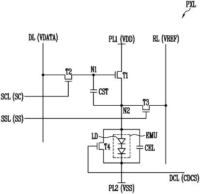
a display panel including a pixel including a light emitting unit including at least one light emitting element; a driving transistor providing a driving current corresponding to a data signal to the light emitting unit; and a first transistor electrically connected between both ends of the light emitting unit; and
a driver that provides the data signal to the pixel and provides a duty control signal to the first transistor,
wherein the driver varies a voltage level of the data signal in a first grayscale section in which a grayscale corresponding to the data signal is greater than or equal to a reference grayscale, and varies a duty ratio of the duty control signal in a second grayscale section in which the grayscale is less than the reference grayscale.
|