| CPC G06V 40/1318 (2022.01) [G02B 27/30 (2013.01); G02F 1/136209 (2013.01); G02F 1/136222 (2021.01)] | 16 Claims |

|
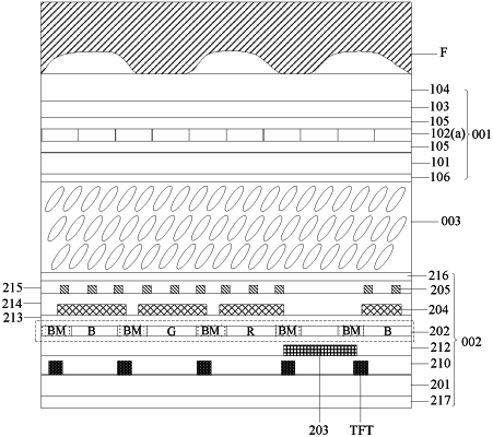
1. A display panel, comprising: an opposing substrate and an array substrate arranged opposite to each other, and a liquid crystal layer located between the opposing substrate and the array substrate, wherein the array substrate comprises:
a first base substrate;
a color film layer, disposed on the first base substrate, wherein the color film layer comprises a black matrix and a plurality of color resistors, the black matrix comprises a plurality of pixel openings and a plurality of first light transmitting holes, and each of the plurality of color resistors is arranged in each of the plurality of pixel openings correspondingly; and
a plurality of photosensitive sensors, disposed between the color film layer and the first base substrate, wherein orthographic projections of the plurality of photosensitive sensors on the first base substrate are in an orthographic projection of the black matrix on the first base substrate, and an orthographic projection of each of the plurality of photosensitive sensors on the first base substrate covers an orthographic projection of at least one of the plurality of first light transmitting holes on the first base substrate;
wherein the opposing substrate comprises: a second base substrate; and a light-shielding layer, disposed on the second base substrate; wherein the light-shielding layer comprises a plurality of second light transmitting holes; and orthographic projections of the plurality of second light transmitting holes on the first base substrate mutually overlap with orthographic projections of the plurality of first light transmitting holes on the first base substrate;
wherein the light-shielding layer comprises: a collimation film attached to the second base substrate; wherein the collimation film is arranged as an entire surface; or an orthographic projection of the collimation film on the first base substrate is in the orthographic projection of the black matrix on the first base substrate;
wherein the collimation film comprises:
a collimation hole layer; and
a flexible basal body layer and a collimating lens layer sequentially disposed on a side facing away from the second base substrate, of the collimation hole layer; wherein
the collimating lens layer comprises: a micro lens array, and a spot area adjustment layer arranged between the micro lens array and the flexible basal body layer;
the collimation hole layer comprises: a plurality of light-shielding parts, and a collimation hole array arranged among the light-shielding parts, wherein the collimation hole array is roughly identical to the micro lens array in distribution, and each collimation hole in the collimation hole array is on a primary optical axis of a corresponding micro lens; and
the collimation holes are the second light transmitting holes, and in a region where the photosensitive sensors are located, orthographic projections of the correspondingly arranged collimation hole, the micro lens and the first light-transmitting hole on the first base substrate overlap with each other.
|