| CPC G06N 3/0464 (2023.01) [G06F 5/16 (2013.01)] | 5 Claims |

|
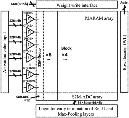
1. An enhanced dynamic random access memory (eDRAM)-based computing-in-memory (CIM) convolutional neural network (CNN) accelerator, comprising four P2ARAM blocks, wherein each of the P2ARAM blocks comprises a 5T1C ping-pong eDRAM bit cell array composed of 64×16 5T1C ping-pong eDRAM bit cells, each of the 64×16 5T1C ping-pong eDRAM bit cells adopts a 5T1C circuit structure and has two 2T read ports, the 2T two read ports are respectively connected to an accumulation bit line (ABL) 1 and an ABL 2, and the 2T two read ports correspond to two activation value input terminals respectively;
the two 2T read ports of the 5T1C ping-pong eDRAM bit cell array support bit cell-based parallel in-memory convolution operations, and the two 2T read ports complete a convolution and a bit line (BL) resetting in parallel in a cycle; and the two 2T read ports operate in a ping-pong mode, wherein one of the 2T read ports performing the BL resetting completes a convolution in a next cycle, the other of the 2T read ports performing the convolution completes a BL resetting in the next cycle, and the 2T read port performing the convolution hides a pre-discharge overhead of a BL;
an eDRAM cell storage node of each of the 5T1C ping-pong eDRAM bit cells is configured to store an analog weight value and a voltage value with a reverse turn-off noise generated by a noise compensation circuit; and when a write transistor of each eDRAM cell storage node is turned off, a forward turn-off noise and the reverse turn-off noise stored in the eDRAM cell storage node are mutually offset, thereby reducing an impact of the noise on an analog weight value stored in the eDRAM cell storage node;
in each of the P2ARAM blocks, 64×2 digital time converters convert a 4-bit activation value into different pulse widths from a row direction and input the pulse widths into the 5T1C ping-pong eDRAM bit cell array for a calculation; a total of 16×2 convolution results are output in a column direction of the 5T1C ping-pong eDRAM bit cell array; and a convolution is realized by charging an input sampling capacitor of a successive approximation register analog-digital converter (SAR ADC) unit by a plurality of 5T1C ping-pong eDRAM bit cells on the ABL at the same time, and a voltage value of the input sampling capacitor is read by the SAR ADC unit;
an input sampling capacitor on an ABL is combined into a SAR ADC unit connected to the ABL, and an area of the input sampling capacitor on the ABL is allotted to a C-DAC capacitor of the SAR ADC unit; every two of 16 columns of 64×16 5T1C ping-pong eDRAM bit cells in the 5T1C ping-pong eDRAM bit cell array form a group; in one group, one column of 64×16 5T1C ping-pong eDRAM bit cells is a sign bit column, and the other column of 64×16 5T1C ping-pong eDRAM bit cells is a numerical bit column; then an ABL 1 and an ABL 2 of the sign bit column each are connected to three SAR ADC units to form an RS ADC unit; an ABL 1 and an ABL 2 of the numerical bit column each are connected to three SAR ADC units to form an RM ADC unit; and 12 related SAR ADC units corresponding to a group of 5T1C ping-pong eDRAM bit unit columns are segmented and crossed, wherein the three RS ADC units connected to the ABL 1 of the sign bit column cross with the three RM ADC units connected to the ABL 1 of the numerical bit column, the three RS ADC units connected to the ABL 2 of the sign bit column cross with the three RM ADC units connected to the ABL 2 of the numerical bit column, and two crossed SAR ADC units are configured to support calculation of a non-2's complement and a 2's complement;
when the 2's complement is calculated, every pair of two crossed RM ADC units and RS ADC units are combined into one ADC for a conversion, where in this case, the sign bit column is used to store a 1-bit sign value, and the numerical bit column is used to store a value of other bits such as five bits; an input sampling capacitor of the RS ADC unit obtains a result of sign bit multiplication, and an input sampling capacitor of the RM ADC unit obtains a result of numerical bit multiplication; and the input sampling capacitor of the RS ADC unit and the input sampling capacitor of the RM ADC unit directly read a 6-bit 2″ 's complement by using the RS ADC unit;
when the non-2's complement is calculated, the RM ADC unit and the RS ADC unit perform conversion independently, wherein in this case, the sign bit column and the numerical bit column are calculated independently, and both the sign bit column and the numerical bit column store a 5-bit non-2's complement; and the RM ADC unit and the RS ADC unit simultaneously read the 5-bit non-2's complement for their respective input sampling capacitors; and
operation control logic and skipping control logic of the SAR ADC unit are tightly coupled in a bit-serial mode to support a cross-layer calculation and an early termination of a convolution layer, an activation function layer, and a maximum pooling layer at the same time.
|