US 11,875,227 B2
Devices and methods for forming optical traps for scalable trapped atom computing
Albert Ryou, Berkeley, CA (US); Mark Stone, Berkeley, CA (US); Matthew Norcia, Berkeley, CA (US); Mickey Mcdonald, Berkeley, CA (US); Brian Lester, Berkeley, CA (US); and Benjamin Bloom, Berkeley, CA (US)
Assigned to Atom Computing Inc., Berkeley, CA (US)
Filed by Atom Computing Inc., Berkeley, CA (US)
Filed on Jun. 12, 2023, as Appl. No. 18/333,437.
Application 18/333,437 is a continuation of application No. PCT/US2023/022780, filed on May 18, 2023.
Claims priority of provisional application 63/343,813, filed on May 19, 2022.
Prior Publication US 2023/0376819 A1, Nov. 23, 2023
Int. Cl. G06N 10/40 (2022.01)
CPC G06N 10/40 (2022.01) 34 Claims
OG exemplary drawing
 
1. A device for forming an optical trap, the device comprising:
a first optical cavity, said first optical cavity configured to form a first standing wave pattern, wherein said first standing wave pattern is two-dimensional;
a second optical cavity, said second optical cavity configured to form a second standing wave pattern, wherein said second standing wave pattern is one-dimensional; and
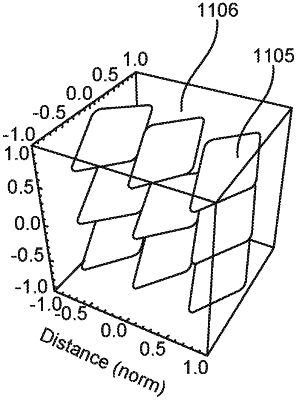
a chamber configured to hold one or more atoms disposed within a three-dimensional array of trapping potentials formed by an overlap between said first standing wave pattern and said second standing wave pattern.