| CPC G06F 3/0625 (2013.01) [G06F 3/0653 (2013.01); G06F 3/0679 (2013.01)] | 20 Claims |

|
1. A non-volatile memory device, comprising:
a control circuit configured to connect to an array of non-volatile memory cells having a NAND architecture and configured to store data in a multi-level cell (MLC) format for the memory cells, the control circuit configured to:
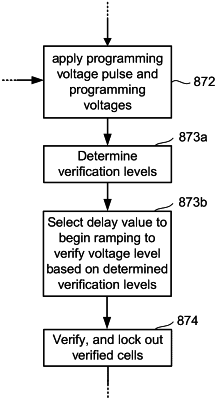
program a selected memory cell of a NAND string connected along a selected word line by applying a series of a plurality of program pulses to the selected word line alternating with a corresponding one or more of a plurality of verify operations for the selected memory cell, where to perform each of the verify operations the control circuit is configured to:
bias the selected word line and unselected word lines connected to the NAND string to an unselected word line read voltage level;
subsequent to biasing the selected word line the unselected word line read voltage level, bias the selected word line to a low voltage level;
determine one or more of a plurality of verify voltage levels;
based on a number of the determined one or more of the verify voltage levels, select a corresponding one of a plurality of delay times; and
subsequent to biasing the selected word line to the low voltage level, sequentially bias the selected word line to the plurality of determined verify voltage levels after waiting the corresponding selected delay time.
|