| CPC G06F 3/0619 (2013.01) [G06F 3/0631 (2013.01); G06F 3/0644 (2013.01); G06F 3/0653 (2013.01); G06F 3/0679 (2013.01)] | 20 Claims |
|
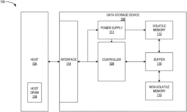
1. A data storage device, comprising:
a memory device; and
a controller coupled to the memory device, wherein the controller comprises a configuration to execute a method for allocating blocks to replace one or more defective blocks in a solid state data storage device, the method comprising:
requesting, with a Flash Translation Layer (FTL), a free block for a first Chip Enable (CE) location from a first free block list responsive to a request to replace a defective block, wherein the first CE location comprises a plurality of NAND group locations;
scanning, with the FTL, the first free block list;
determining that the free block is not available from the first free block list to replace the defective block, wherein:
the first free block list is refilled from a queue of free blocks from an unallocated block pool storing a plurality of free blocks from a plurality of dies of the memory device, wherein the first free block list is a subset of the unallocated block pool and distinct from the unallocated block pool; and
refilling the first free block list comprises selecting a free block from the unallocated block pool that has a same CE location as a free block allocated from the free block list to refill the free block list;
determining that the free block is available from the unallocated block pool to replace the defective block;
replacing the defective block with the free block allocated from the unallocated block pool when the free block is available from the unallocated block pool, wherein the defective block remains in a read-write mode;
allocating the free block responsive to receiving a write command for the first CE location; and
programming data to the allocated free block, wherein the data is associated with the write command.
|