| CPC G06F 3/04164 (2019.05) [G06F 3/045 (2013.01); G06F 3/0445 (2019.05); G06F 2203/04107 (2013.01)] | 20 Claims |
|
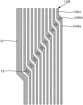
1. A touch substrate, comprising a touch area and a peripheral area surrounding the touch area, wherein the touch substrate further comprises a touch electrode and a touch signal line that are coupled to each other; at least portion of the touch electrode is located in the touch area;
at least portion of the touch signal line is located in the peripheral area, the touch signal line comprises at least one corner portion, each of the at least one corner portion comprises a first part, a second part and a third part that are connected end to end in sequence, an extension direction of the first part is the same as an extension direction of the third part, and an extension direction of the second part intersects with the extension direction of the first part; and
a width of the second part in a direction perpendicular to the extension direction of the second part is larger than a width of the first part in a direction perpendicular to the extension direction of the first part, and is larger than a width of the third part in a direction perpendicular to the extension direction of the third part,
wherein the touch signal line comprises a first conductive layer and a second conductive layer arranged in different layers: the second part is arranged on each of the first conductive layer and the second conductive layer, and the second part arranged on the first conductive layer is coupled to the second part arranged on the second conductive layer.
|