| CPC G06F 3/04164 (2019.05) [G06F 3/0412 (2013.01); G06F 3/0443 (2019.05); G06F 3/0446 (2019.05); G09F 9/30 (2013.01); G09G 2300/0413 (2013.01)] | 20 Claims |
|
1. A display panel, comprising:
a base substrate, the base substrate comprising a display region and a non-display region outside the display region;
a touch electrode on the base substrate, the touch electrode being located within the display region; and
a plurality of signal lines electrically connected with the touch electrode, the plurality of signal lines being distributed within the non-display region,
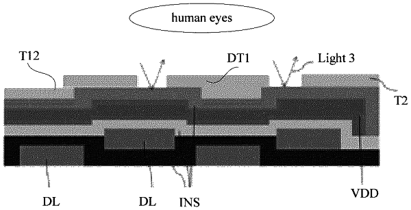
wherein the non-display region comprises a light reflective uneven region, the light reflective uneven region comprises a reflective material layer on the base substrate, the reflective material layer comprises an uneven surface facing away from the base substrate,
wherein the display panel further comprises a light reduction structure within the non-display region, the light reduction structure is above the reflective material layer and at least configured to reduce light reflected from the uneven surface of the reflective material layer, and
wherein the light reduction structure is separated from the plurality of signal lines and the touch electrode.
|