| CPC G06F 3/0412 (2013.01) [G02F 1/1334 (2013.01); G02F 1/13338 (2013.01); G02F 1/133616 (2021.01); G02F 1/136286 (2013.01); G06F 3/0445 (2019.05); G06F 3/0446 (2019.05); G06F 3/04166 (2019.05); G09G 3/3611 (2013.01); G06F 2203/04108 (2013.01); G09G 2300/023 (2013.01); G09G 2300/0426 (2013.01); G09G 2310/08 (2013.01); G09G 2340/12 (2013.01)] | 16 Claims |
|
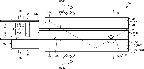
1. A sensor-equipped display device comprising:
an array substrate;
a counter substrate;
a first sensor configured to detect a first detection-target object close to the counter substrate;
a second sensor configured to detect a second detection-target object close to the array substrate,
a cover glass bonded to the counter substrate;
a liquid crystal layer between the array substrate and the counter substrate; and
a light source disposed so as to emit light into a side surface of the cover glass and a side surface of the counter substrate, wherein
a first background of the array substrate is viewed from outside the counter substrate, and a second background of the counter substrate is viewed from outside the array substrate,
the cover glass is located between the counter substrate and the first sensor,
the second sensor is provided to the array substrate,
the array substrate comprises a plurality of pixel electrodes each disposed in a corresponding one of pixels and holding capacitance electrodes at least partially overlapping the pixel electrodes in a plan view with an inorganic insulating layer interposed between the holding capacitance electrodes and the pixel electrodes, and
the holding capacitance electrodes are divided by slits and serve as drive electrodes of the second sensor.
|