| CPC G06F 3/0412 (2013.01) [G06F 1/3203 (2013.01); G06F 1/3265 (2013.01); G06F 3/04883 (2013.01); G02F 1/13338 (2013.01); Y02D 10/00 (2018.01)] | 17 Claims |
|
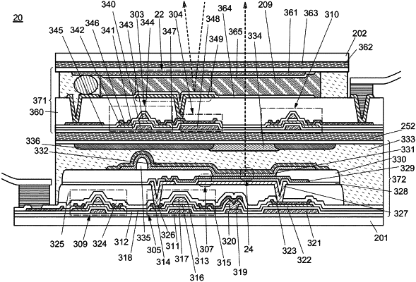
1. A display device comprising:
a flexible substrate;
a first insulating layer over the flexible substrate;
a first semiconductor layer over the first insulating layer;
a first conductive layer functioning as one of a source electrode and a drain electrode of a first transistor, the first conductive layer being in contact with a top surface of the first semiconductor layer;
a second insulating layer over the first semiconductor layer;
a second conductive layer over the second insulating layer;
a third conductive layer over the second insulating layer;
a second semiconductor layer over the second insulating layer;
a third insulating layer over the second semiconductor layer;
a fourth conductive layer over the third insulating layer, the fourth conductive layer functioning as a gate electrode of a second transistor;
a fourth insulating layer over the fourth conductive layer;
a first electrode layer of a display element over the fourth insulating layer; and
a second electrode layer of the display element over the first electrode layer,
wherein the first conductive layer overlaps with the second conductive layer, the third conductive layer, the fourth conductive layer, and the second semiconductor layer,
wherein the first semiconductor layer comprises silicon, and
wherein the second semiconductor layer comprises an oxide semiconductor.
|