| CPC G06F 11/1441 (2013.01) [G06F 11/076 (2013.01); G06F 11/0742 (2013.01); G06F 11/0793 (2013.01); G06F 11/141 (2013.01); G06F 3/0679 (2013.01); G06F 2201/82 (2013.01); H04M 2201/36 (2013.01); H04M 2250/22 (2013.01)] | 17 Claims |

|
1. A flash memory control apparatus comprising:
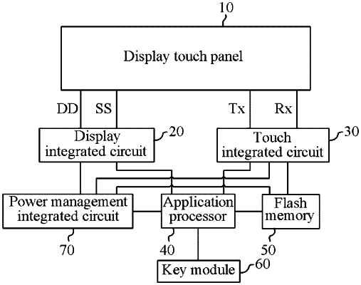
a flash memory circuit including a first hold signal terminal for receiving a hold signal and a first chip select signal terminal for receiving a chip select signal, and configured to store and provide flash data; and
an application processor including a second hold signal terminal for providing the hold signal and a second chip select signal terminal for providing the chip select signal and configured to reset, when it is determined, on the basis of error information, that an abnormal case due to a read error for the flash data has occurred more than a predetermined number of times,
wherein the flash memory circuit resets the flash data by the hold signal and the chip select signal for resetting,
the flash memory circuit provides the flash data in response to a read request of a touch integrated circuit or a display integrated circuit, and
the application processor receives the error information on the read error for the flash data from the touch integrated circuit or the display integrated circuit.
|