| CPC G05F 3/24 (2013.01) [G05F 1/575 (2013.01); H03F 3/45475 (2013.01)] | 20 Claims |
|
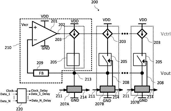
1. A circuit comprising:
a first load circuit coupled between a first node and a reference voltage node, wherein an input terminal of the first load circuit is configured to receive a first input signal;
a first transistor coupled between a voltage supply node and the first node;
a second load circuit coupled between the first node and the reference voltage node, wherein an input terminal of the second load circuit is configured to receive a second input signal;
a second transistor and a second switch coupled in series between the voltage supply node and the first node; and
an amplifier, wherein a first input terminal of the amplifier is configured to be coupled to a reference input voltage, and a second input terminal of the amplifier is coupled to the first node through a feedback network, wherein an output terminal of the amplifier is coupled to a first gate terminal of the first transistor and a second gate terminal of the second transistor, wherein the second switch is configured to be opened and closed alternately during normal operation of the circuit, wherein during the normal operation of the circuit, the second switch is configured to be closed by a control signal for a period of time when a rising edge or a falling edge is detected in the second input signal.
|