| CPC G02F 7/00 (2013.01) [G02F 1/0305 (2013.01); G02F 1/0327 (2013.01); G02F 2202/105 (2013.01); G02F 2202/20 (2013.01)] | 3 Claims |

|
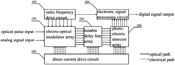
1. A monolithically integrated optical analog-to-digital conversion system based on a lithium niobate-silicon wafer, comprising
an electro-optical modulator array (100),
a tunable delay line array (200),
a photoelectric detector array (300),
a radio-frequency drive circuit (400),
a direct-current drive circuit (500), and
an electronic signal processing circuit (600),
wherein the electro-optical modulator array (100), the tunable delay line array (200), the photoelectric detector array (300), the radio-frequency drive circuit (400), the direct-current drive circuit (500), and the electronic signal processing circuit (600) are integrated on a single chip;
the electro-optical modulator array (100) receives an optical pulse and analog signal input from an outside out of the monolithically integrated optical analog-to-digital conversion system, and completes sampling of the analog signal and time-division demultiplexing of the optical pulse to form 2n paths of optical outputs under the drive of the radio-frequency drive circuit (400) and the direct-current drive circuit (500);
the electro-optical modulator array (100) comprises 2n lithium niobate-silicon electro-optical modulators, one of which is a sampling gate (101) for receiving the analog signal input;
the sampling gate (101) is a single-output electro-optical modulator with only one optical output port, and the other 2n−1 electro-optical modulators form an n-level time-division demultiplexing structure (102), and each of the other 2n−1 electro-optical modulators is a double-output electro-optical modulator with one optical input port and two optical output ports, and n-th level electro-optical modulators of the n-level time-division demultiplexing structure have 2n optical output ports;
the tunable delay line array (200) comprises 2n tunable delay lines positioned behind the 2n optical output ports of the electro-optical modulator array (100), respectively; each of the 2n tunable delay lines comprises an optical input port and an optical output port; and each of the 2n optical output ports of the n-th level electro-optical modulators of the n-level time-division demultiplexing structure (102) is connected to a corresponding optical input port of the 2n tunable delay lines;
the photoelectric detector array (300) comprises 2n silicon-germanium photoelectric detectors positioned behind the 2n optical output ports of the 2n tunable delay lines, respectively; each of the 2n silicon-germanium photoelectric detectors comprises an optical input port and an electrical signal output port; and each of the optical output ports of the 2n tunable delay lines is connected to a corresponding optical input port of the 2n silicon-germanium photoelectric detectors;
the radio-frequency drive circuit (400) comprises a clock (401), a frequency multiplier group (402), a frequency divider group (403), a filter group (404), and a phase shifter group (405) for providing the time-division demultiplexing structure of the electro-optical modulator array (100) with radio-frequency drive and the electronic signal processing circuit (600) with clock signals;
the direct-current drive circuit (500) comprises a tunable voltage source group (501) and a direct-current power source group (502) for controlling a bias voltage of each electro-optical modulator in the electro-optical modulator array (100) to provide the tunable delay line of the tunable delay line array (200) with direct-current and to provide each photoelectric detector of the photoelectric detector array (300) with a power source;
the electronic signal processing circuit (600) comprises a trans-impedance amplifier group (601), an electronic analog-to-digital converter group (602), and a digital signal processor (603), sequentially, the trans-impedance amplifier group (601) converts current signals output by the photoelectric detector array (300) into voltage signals, amplifies the voltage and inputs to the electronic analog-to-digital converter group (602), the electronic analog-to-digital converter group (602) quantizes the voltage and then outputs digital signals for the digital signal processor (603), and the digital signal processor (603) outputs the digital signals as an output of the monolithically integrated optical analog-to-digital conversion system after completing channel interleaving processing;
wherein the optical pulse input is connected to an optical input port of the sampling gate (101);
the analog signal is input through an electrical input port of the sampling gate (101);
the only one optical output port of the sampling gate (101) is connected to an optical input port of a first-level electro-optical modulator of the 2n−1 electro-optical modulators of the n-level time-division demultiplexing structure (102);
2n−1 radio-frequency output ports of the radio-frequency drive circuit (400) are correspondingly connected to electrical input ports of the 2n−1 electro-optical modulators of the n-level time-division demultiplexing structure (102);
the 2n electrical signal output ports of the photoelectric detector array (300) are correspondingly connected to 2n electrical signal input ports of the electronic signal processing circuit (600);
a clock signal output end of the radio-frequency drive circuit (400) is connected to a clock input port of the electronic signal processing circuit (600);
voltage outputs of the direct-current drive circuit (500) are connected to the sampling gate (101), the 2n−1 electro-optical modulators of the n-level time-division demultiplexing structure (102), the tunable delay line array (200), and a direct-current input port of the photoelectric detector array (300), respectively; and
an electrical output port of the electronic signal processing circuit (600) is an output port of the system, and n≥2.
|