| CPC G02F 1/134309 (2013.01) [G02F 1/13439 (2013.01); G02F 1/133512 (2013.01); G09G 3/3614 (2013.01); G09G 2300/0426 (2013.01); G09G 2320/0233 (2013.01); G09G 2360/144 (2013.01)] | 16 Claims |
|
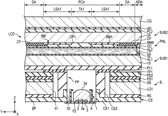
1. An electronic device, comprising:
a liquid crystal panel; and
a camera,
the liquid crystal panel including a display area and an incident light control area,
the camera overlapping the incident light control area,
the display area including a pixel electrode,
the incident light control area including a first control electrode which is different in shape from the pixel electrode, a second control electrode, and a common electrode,
a voltage applied to the first control electrode and a voltage applied to the second control electrode being different in polarity from a common voltage applied to the common electrode.
|